Advanced Chip Analysis, Microscopy & Circuit Editing
Unlock precision and insight for your integrated circuit projects with our advanced laboratory services. From failure analysis and FIB circuit modification to high-resolution electron microscopy, ADVANCED CIRCUIT ENGINEERS SERVICES, INC delivers cutting-edge microelectronic support trusted by the semiconductor, AI system, and automotive industries.
Our Core Services
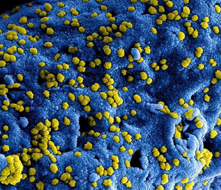
Dual-Beam FIB-SEM Microscopy
Advanced imaging of micro and nanoscale structures using focused ion beam/scanning electron microscopy (FIB-SEM). Analyze device cross-sections with unparalleled detail for defect inspection, structural analysis, and process validation across semiconductor, automotive, and AI hardware.
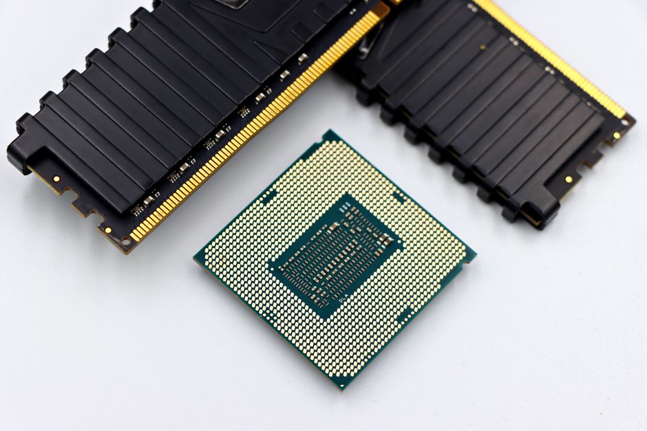
Transmission Electron Microscopy (TEM)
Ultra-high resolution imaging at the atomic scale with advanced TEM techniques. Reveal phase, grain, and interface properties in nanoelectronics and devices. Our lab provides precise lamella preparation, nanoanalysis, and fast turnaround for R&D and failure investigation.

FIB Circuit Edit & Modification
Implement design changes directly on fabricated ICs. Our focused ion beam (FIB) circuit editing enables precise rerouting, open or short fixes, and real-time design debug. Access rapid turnaround without going back to photomask revisions—vital for time-sensitive development.
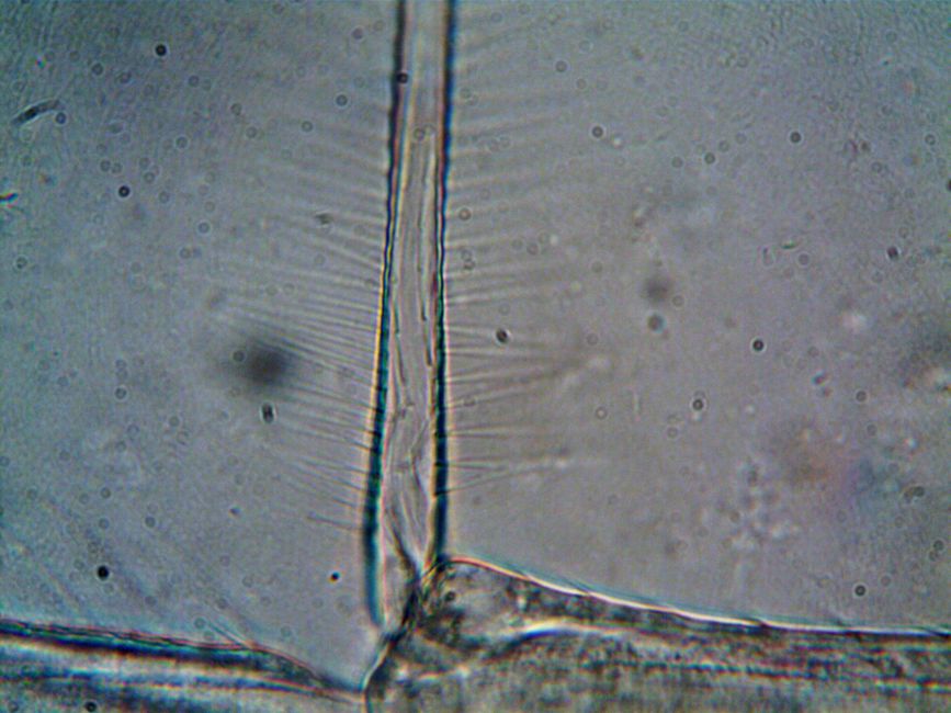
Failure Analysis
Comprehensive root cause determination for electronic and semiconductor failures. Methods include electrical probing, microscopy, and spectroscopic diagnostics. Whether facing yield loss, performance drift, or intermittent errors, our team uncovers actionable insight to drive corrective action.
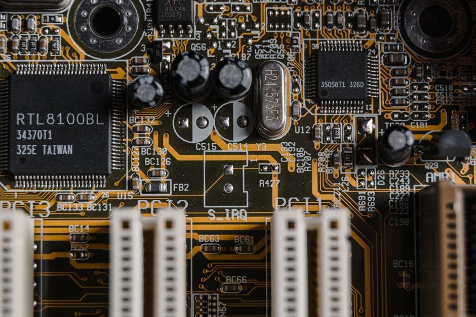
Advanced Spectroscopy
Material characterization at the elemental and molecular level through a variety of spectroscopy approaches—EDS, EELS, and more. Verify composition, contamination, or failure modes in microchips and system-level assemblies to support qualification and compliance.
IC Testing & Validation
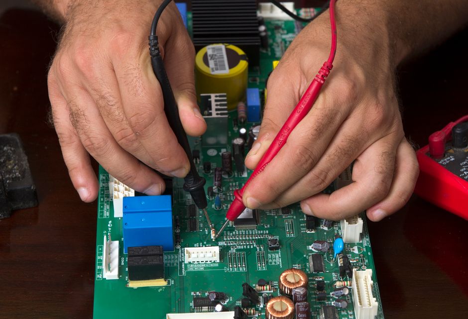
Precise electrical validation of ICs and system components. Utilize probe stations, test benches, and measurement equipment to ensure compliance, performance, and reliability before deployment in mission critical applications like AI or automotive electronics.
Industries & Clients
- Semiconductor Manufacturers: Accelerate new process development, solve device defects quickly, and reduce time to market.
- AI System Designers: Ensure reliability, performance, and rapid iteration for state-of-the-art AI hardware.
- Automotive Electronics: Validate chips for automotive safety, robustness, and compliance with functional safety standards.
- Research & Academia: Access high-resolution imaging and failure analysis tools for advanced studies of new materials and integrated circuits.
- Systems Integrators: Debug boards, analyze interconnects, and verify assemblies pre- and post-field deployment.
How to Select the Right Service
Project Preparation Checklist
- Sample Cleanliness: Ensure devices are free of debris and handled according to ESD safety standards.
- Documentation: Provide current schematics, failure reports, and suspected problematic regions.
- Packaging/Shipping: Package fragile ICs or samples carefully to prevent physical damage in transit.
- Clear Communication: Include contact info for your technical lead to enable rapid clarification during processing.
How to Work With Us
About ADVANCED CIRCUIT ENGINEERS SERVICES, INC
ADVANCED CIRCUIT ENGINEERS SERVICES, INC is dedicated to providing industry-leading analytical and modification solutions for advanced integrated circuits and systems. With expertise covering failure analysis, focused ion beam (FIB) circuit editing, and state-of-the-art electron microscopy, we support innovation and reliability in semiconductors for AI, automotive, and the broader electronics sector.
Our laboratory combines precision instrumentation, deep technical knowledge, and a commitment to confidentiality. We partner with our clients from consultative project planning through to robust reporting and corrective action support.
Contact Us
- Phone: +1 (408) 719-1278
- Email: info@arab-engineerng.com
- Document: 3691649
For technical enquiries, project submissions, or consultation, please email or call us. Our experienced engineers help assess your needs and propose the most effective analytical pathway. We respond promptly, typically within the next business day.
Office Address:
308 South Abbott Ave
Milpitas, CA 95035